By transfer-printing tiny LEDs instantly above nanowire emitters, researchers confirmed a compact path to electrically managed, chip-scale photonic techniques, although additional optimization is required earlier than sensible deployment.

Schematic movement diagram exhibiting the fabrication strategy of the nanowire system with transfer-printed micro-LED units.
A analysis paper lately revealed within the journal Nanotechnology demonstrated the usage of transfer-printed micro-light-emitting diode (LED) units as single, built-in nanowire excitation sources for nanowire emitters.
Scalable Nanowire-based Methods
Over the past decade, analysis on nanowire emitters has made important progress towards scalable nanowire photonic built-in circuitry (PIC), advancing from device-level investigations to system-level demonstrations. Presently, the main target of analysis is shifting in direction of addressing the scalability of superior circuitry and inter-device variability.
The mixing of nanowire expertise into photonic circuitry is an lively subject of analysis, as the problems plaguing nanowire-based system improvement prolong past gadget variability.
Heterogeneous and hybrid integration strategies are appropriate for assembling nanowire techniques, as they supply flexibility in substrate and materials choice and allow the switch of each rising and mature gadget applied sciences into photonic circuitry.
But, this integration method incurs trade-offs in positioning accuracy, scalability, and time. Equally, micro-tip-based techniques face important scalability challenges and require substantial time for gadget alignment and launch/seize.
Micro-stamp-based strategies, reminiscent of micro-transfer printing, can obtain serial integration speeds of over 1 gadget/minute at 500 nm integration accuracy. This integration methodology is often used for micro-/mini-LED and PIC meeting.
Scalable strategies for nanowire detection and excitation are additionally essential for transitioning this expertise from laboratory demonstrations to real-world sensible functions. Thus, exploring routes for individually addressable and in-parallel excitation of nanowire emitters is crucial.
Earlier research have displayed the potential of micro-LED-on-complementary metal-oxide-semiconductor (CMOS) expertise for optically thrilling embedded nanowire circuitry. This scalable excitation method permits independently addressable nanowire arrays with on/off-key modulation within the 100 MHz vary by projecting micro-LED mild patterns instantly onto nanowire techniques.
The Switch-printed Micro-LED-based Strategy
Based mostly on advances in micro/mini-LED expertise, which is now extensively utilized in optogenetics and visible-light communications, researchers on this work introduced a method for scalable electro-optical on-chip addressing of semiconductor nanowire emitters utilizing transfer-printed micro-LEDs.
Within the proposed method, the pumping components have been instantly built-in on high of the nanowire circuitry, permitting small-signal modulation at tens of MHz charges and electro-optical addressing of nanowires.
This technique additionally diminished the shape issue of nanowire-based techniques, opening the best way to realizing programmable nanowire PICs with out requiring nanowire post-processing or complicated fabrication steps and bringing nanowire-based techniques nearer to chip-scale fabrication compatibility.
On this work, indium phosphide (InP) nanowire semiconductor nanoemitters with diameters of ~500 nm and lengths of 5–7 µm have been used. They exhibited a excessive quantum effectivity of ~50% and supported room-temperature emission at a central wavelength of ~860 nm.
After progress, the nanowires have been mechanically transferred onto host-circuitry substrates utilizing bespoke tender microstamps, reaching sub-500 nm positioning accuracy by way of superior alignment protocols. To reinforce mode overlap with SU-8 6005 polymer waveguides, the nanowires have been positioned into waveguide cavities through a multi-step fabrication course of.
In parallel, micro-LED membranes have been fabricated from indium gallium nitride (InGaN) LED epitaxial buildings grown on silicon (Si) substrates, consisting of a 200 nm aluminum nitride (AlN) layer, a 950 nm aluminum-graded GaN buffer, an 800 nm n-type-GaN layer, a 100 nm multi-quantum properly area, and a 140 nm p-type-GaN layer.
Optoelectronic characterization was carried out utilizing a 3-axis positioning stage with electrical probes driving the micro-LEDs, whereas free-space optics enabled imaging, alignment, and waveguide side assortment. After probe alignment, the setup was simplified, and additional optimization was proposed through wire bonding and ceramic chip integration.
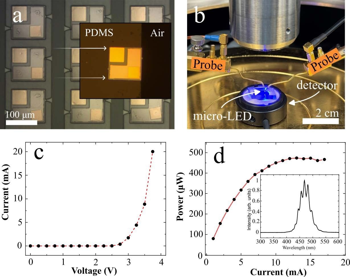
Micrograph exhibiting suspended micro-LED array. Inset reveals a micro- LED pixel heterogeneously built-in on the fringe of a PDMS substrate. (b) Electrically probed micro-LED pixel on PDMS substrate, on a probing station. (c) I-V curve of the micro-LED-on-PDMS pixel. (d) Optical energy measurement of the pixel with saturation area at round 10 mA. Inset reveals the electro-luminescence spectrum of a consultant micro-LED gadget.
Viability of the Strategy
The findings demonstrated that particular person waveguide-coupled nanowires exhibited small-signal modulation within the tens of MHz vary at room temperature. Micro-LED integration with nanowire emitters on a chip enabled localized, scalable excitation with out exterior optics.
The 470 nm emission from the micro-LEDs was absorbed by the nanowire gadget, which subsequently radiated near-infrared mild at a central wavelength of roughly 860 nm as reported beforehand. Attributable to excessive divergence, the optical overlap between the LED emission space and the nanowire area was estimated to be under 1%.
With a measured energy density of roughly 90 nW/µm², the optical energy projected onto the nanowire was estimated at round 300 nW. This resulted in diminished quantum effectivity in contrast with typical pulsed laser excitation on account of decrease pump energy and the emission regime of the nanowire units.
The authors additionally reported that the depth measured on the waveguide side from units with nanowire emitters was roughly 2–3 instances greater than that from naked waveguides, primarily based on measurements from seven waveguide-integrated nanowire units. To reduce unintended excitation of polymeric SU-8 waveguides, overlap with the built-in LED was diminished throughout alignment and printing by constraining geometry and protection. Time-domain measurements over 20–120 MHz have been filtered with a Savitzky–Golay filter to take away high-frequency noise.
To enhance excitation fluence, the authors instructed introducing a meta-surface lens layer between the LEDs and the nanowire system to reinforce mild focusing and pumping effectivity. In conclusion, this examine’s findings demonstrated the feasibility of the proposed method for realizing programmable high-density nanowire networks, though additional optimization is required to transition the platform from a preliminary demonstration to sensible functions.